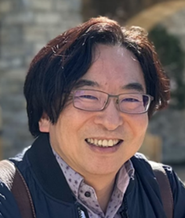
#1: Chip-Backside Vulnerability to Intentional Electromagnetic Interference in Integrated Circuits
Prof. Makoto Nagata, Kobe University, Japan
Monday, 7 October, 9:10-9:40
Abstract
The backside of integrated circuits (ICs) in flip-chip assembly is susceptible to intentional electromagnetic interference due to its open surface. In this article, we propose a model in which conducted current noise from a localized area of the Si substrate on the chip-backside causes errors in complementary metal-oxidesemiconductor (CMOS) digital circuits. This model explains for the first time the mechanism of bit-flip errors in bistable circuits caused by high-voltage pulse (HVP) injection on the backside of the IC. The injected current from the backside of the IC not only flows into the power distribution network, but also charges the gate capacitance of the next stage via p–n junction diodes of body/drain or body/source in N-channel MOSFETs (NMOS) with twin-well structures, resulting in bit-flip errors. In this study, circuit simulations were performed using a three-dimensional RC network model of the IC chip and an HVP injector. These simulations have shown that the P-well voltage is biased depending on the arrangement of the tap cells, reproducing bit-flip errors in the bistable circuit of a D flip-flop. The simulation results were validated on a fabricated prototype IC chip, which confirmed the trend of data dependency for errors related to the physical layout.

Presenter’s biography
Makoto Nagata received the B.S. and M.S. degrees in physics from Gakushuin University, Tokyo, in 1991 and 1993, respectively, and a Ph.D. in electronics engineering from Hiroshima University, Hiroshima, in 2001. He is currently a full professor with the graduate school of science, technology and innovation, Kobe University, Kobe, Japan.
He chaired the technology directions subcommittee for ISSCC (2018-2022) and now serves as its executive committee member. He was the technical program chair (2010–2011), the symposium chair (2012–2013), and an executive committee member (2014–2015) for the symposium on VLSI circuits. He was the IEEE Solid-State Circuits Society (SSCS) AdCom member (2020-2022), the distinguished lecturer (2020-2021 and 2024-present) and the chapters vice chair (2022-present) of the society.
#2: Modelling and Design of Highly EMI Immune CMOS OpAmp Topologies
Dr. Subrahmanyam Boyapati, Synopsis, Ireland
Tuesday, 8 October, 9:10-10:00
Abstract
This paper gives a review of the modeling and design of CMOS Miller operational amplifier (OpAmp) and folded cascode operational amplifier that has high immunity to electro-magnetic interference (EMI). The highly EMI immune CMOS OpAmps and folded cascode OpAmps has unique features, such as compact power and low output offset voltage, when compared to the classical Miller OpAmp and the classical folded cascode OpAmps in the literature. The output offset current modeling equations are derived for the CMOS OpAmps including the body effect and channel length modulation. The CMOS OpAmps uses the replica concept along with the source-buffered technique in order to achieve high EMI immunity across a wide range of frequencies (10 MHz to 1 GHz). The highly EMI immune CMOS OpAmps are designed using the first-order quadratic mathematical model. The circuit has been fabricated/designed using 0.18 μm mixed-mode CMOS technology. The performance result shows that the maximum EMI-induced input offset voltage for the CMOS OpAmps is less than 5 mV over a wide frequency range from 1 MHz to 1 GHz, which is lower when compared to the available classical Miller OpAmps and the folded cascode OpAmps.

Presenter’s biography
Subrahmanyam Boyapati received the MTech. degree in integrated electronics and circuits from the Indian Institute of Technology (IIT), Delhi, New Delhi,India, in 2006, and the Ph.D. degree in microelectronics from the IITB-Monash Research Academy, IIT Bombay, Mumbai, India, in 2017. He is a recipient of the Prime Minister’s Fellowship Scheme for Doctoral Research, a public–private partnership between the Science and Engineering Research Board, Department of Science and Technology, Government of India, and Confederation of Indian Industry. From 2018 to 2021, he was an Analog Design Engineer with Intel-Bangalore where he worked on high-speed receiver design for High Bandwidth Memory (HBM) applications. From 2001 to May 2024, he was a Key Researcher with the Center for Integrated Systems and Circuits Design, Carinthia University of Applied Sciences, Austria. Currently he is working as a Senior Staff Analog Design Engineer with Synopsys, Dublin, Ireland. His current research interests include analog and mixed signal integrated circuit design for sensor and biomedical applications, integrated circuit design with a high robustness to electromagnetic interference and high-speed receiver design circuits for the ADCs.
#3: Common Mode Noise Reduction Methods Used for High Power Density DC/DC Converters
Prof. Jun Imaoka, Nagoya University, Japan
Wednesday, 8 October, 9:10-10:00
Abstract
Compound power semiconductor devices, such as Silicon Carbide (SiC) and Gallium Nitride (GaN), are widely adapted into automotive, renewable energy, and energy management applications to achieve carbon neutrality. These devices can operate at higher frequencies compared to Silicon (Si)-based devices due to their high switching speed and low on-resistance. Furthermore, high-frequency operation contributes to the realization of high power density in DC/DC converters. However, with the widespread application of compound semiconductor devices capable of high-frequency operation, the importance of common mode noise reduction is significantly increasing. Therefore, this paper introduces state-of-the-art technologies for common-mode noise reduction based on a literature review. Primarily, this paper presents methods for common mode noise reduction in high-power and high-frequency applications without increasing the converter’s volume.

Presenter’s biography
JUN IMAOKA (Member, IEEE) received the M.S. and Ph.D. degrees in electronic function and system engineering from Shimane University, Matsue, Japan, in 2013 and 2015, respectively. From October 2015 to March 2018, he was an Assistant Professor with Kyushu University, Fukuoka, Japan. From April 2018 to March 2021, he was an Assistant Professor with Nagoya University, Nagoya, Japan. He is currently an Associate Professor with the Institute of Materials and Systems for Sustainability (IMaSS), Nagoya University. His research interests include the design of integrated magnetic components, modeling for high-power-density power converters, thermal management for power converters, magnetic material application, and EMI of switching power supply.
