#1: IEC standardized IC EMC test methods: application guidance
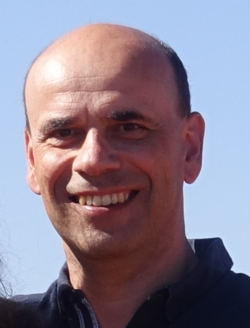
Dr. Frank Flotz, Infineon Technologies, Germany
Monday, 7 October, 13:00-14:30
Abstract
The tutorial provides in the first part an overview of the current IEC EMC standards for integrated circuits, informs about ongoing and planned standardization projects and gives an outlook on the IC EMC standardization roadmap also with reference to relevant standardization activities in the automotive area at ISO and CISPR. The second part presents and discusses the approach and application of selected IC EMC measurement methods according to the Generic IC EMC Test Specification of the ZVEI.

Presenter’s biography
Frank Klotz, studied electrical engineering at the Technical University of Ilmenau, where he received his PhD in the field of EMC of power semiconductor topologies. In 1996 he started his career in the semiconductor division of Siemens AG, now Infineon Technologies AG. Today he is head of Infineon’s EMC organization, chair of IEC SC47A Integrated Circuits and member of the EMC standardization committees at IEC, CISPR and ISO.
#2: How signal and power integrity influence the silicon device integration in the package and system
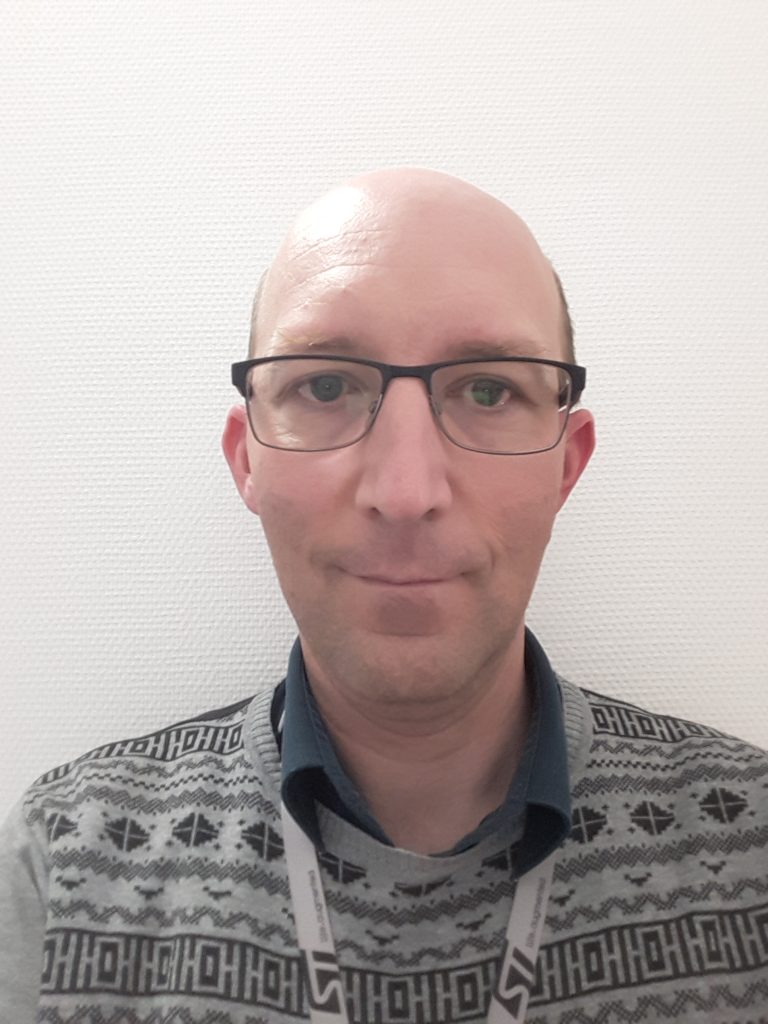
Olivier Bayet, STMicroelectronics Grenoble, France
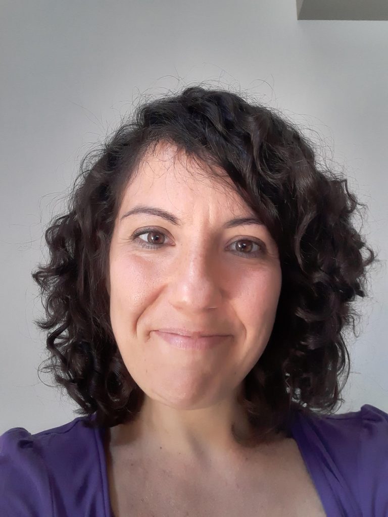
Aurora Sanna, STMicroelectronics Agrate Brianza, Italy
Tuesday, 8 October, 13:00-14:30
Abstract
In the context of integrated circuits development, signal and power integrity (SI & PI) optimization is key to ensure the required electrical performances. With the increasing operating frequencies, decreasing voltage levels and increasing power consumption, package interconnections assume a significant weight and the interaction between chip, package and board needs a deep assessment through a co-design and co-simulation approach. The proposed tutorial goes through the overall design process to optimize signal and power integrity, from pre-layout strategy definition to post-layout verification, with a strong focus on package interconnections technology and design. The importance of chip-package co-design is underlined and a constant link between design, electromagnetic modeling and simulations is maintained, to validate each step of the process.
Main topics:
- Pre-layout strategy for SI and PI optimization
- Die-package-board integration constraints
- Package technology selection based on physical and electrical constraints
- Package routing strategy definition with the support of simulation
- Design partitioning, smart routing strategy definition based on layout symmetries
- Layout optimization and verification for SI and PI
- Signal integrity simulations, from package-level to system-level (frequency-domain and time-domain, input models requirements)
- Power integrity simulations, from package-level to system-level (DC and AC, frequency domain and time-domain, input models requirements, decoupling capacitors selection)
- Link between SI, PI and thermal for accurate analysis
- Link between SI/PI and electromagnetic emissions
- Output chip/package models
Presenters’ biography

Olivier Bayet is Senior Member of Technical Staff at STMicroelectronics and has over 24 years of experience in design and EDA for IC and package. He developed new methods for voltage drop analysis, IC-package co-design and its associated physical and electrical verification. As part of the mobile platform and later networking processor design teams, Olivier setups the design and verification process for SoC-Package-PCB co-design to enable complex interfaces such as LPDDR, DDR, SerDes. Currently Olivier is leading the die/package co-design for various types of projects in the RF & Communication division of ST covering the signal integrity analysis of RF links, antennas, high speed serial links and the system power integrity analysis of low voltage and high-power consumption devices. Olivier holds an MSEE from ENSERB, Bordeaux, France.

Aurora Sanna got the master’s degree in Electronics Engineering at Politecnico di Milano, in 2011. Since then, she has worked in the field of electrical modeling of interconnections, starting from PCBs and then moving to IC-packages, dealing with Signal Integrity, Power Integrity and Electromagnetic Compatibility problems. Currently, she is part of Back-end Manufacturing and Technology RnD group in STMicroelectronics and she is leader of a team dedicated to package design, electrical modeling and thermal modeling. She is member of STMicroelectronics Technical Staff.
